Fermi Level Expression In Intrinsic Semiconductor Is - Fermi Energy In Intrinsic Semiconductor / Example 11 silicon crystal is doped with atoms per m.. Intrinsic conductivity in semiconductor, the electrons and holes will participate in electrical conductivity. Fermi level lies in the midway between the valence band top and conduction band bottom of an intrinsic semiconductor, as shown in fig. Ec is the conduction band. Therefore, the fermi level for the intrinsic semiconductor lies in the middle of band gap. The electrical conductivity of the semiconductor depends upon.
At absolute zero temperature intrinsic semiconductor acts as perfect insulator. The fermi level lies between the valence band and conduction band because at absolute zero temperature the electrons are all in the lowest energy state. By substituting the carrier densities by their respective expressions, this relationship allows defining the fermi level for an intrinsic semiconductor e fi. Consequently, we see from this equation that the fermi level should typically lie very close to the middle of the energy gap in intrinsic semiconductors. So at absolute zero they pack into the lowest available energy states and build up a fermi sea of electron.
Semiconductor Applications L 3 1 Lecture 3 Electrons from slidetodoc.com The fermi level represents the energy state with a 50% probability of being filled if no forbidden band exists,.i.e., if e = e f then f(e)=1/2 for any value of temperature. The electrical conductivity of the semiconductor depends upon. Example 11 silicon crystal is doped with atoms per m. Fermi level represents the average work done to remove an electron from the material (work function) and in an intrinsic semiconductor the electron and hole concentration are equal. The added impurity is very small, of the order of one atom. Therefore, the fermi level for the intrinsic semiconductor lies in the middle of forbidden band. So at absolute zero they pack into the lowest available energy states and build up a fermi sea of electron. (18) is of the order of 1 ev, while the second is of the order of a few tens of millielectron volts at 300 k.
The probability of occupation of energy levels in valence band and conduction band is called fermi level.
Fermi level of extrinsic semiconductor extrinsic semiconductors are formed by adding suitable impurities to the intrinsic semiconductor. The intrinsic fermi energy is typically close to the midgapenergy, half way between the conduction and valence band edge. Kb is the boltzmann constant. Labeling the fermi energy of intrinsic material as e i, we can then write two relations between the intrinsic carrier density and the intrinsic fermi energy, namely: Intrinsic conductivity in semiconductor, the electrons and holes will participate in electrical conductivity. The added impurity is very small, of the order of one atom. So at absolute zero they pack into the lowest available energy states and build up a fermi sea of electron. Ec is the conduction band. Fermi level expression in intrinsic semiconductor is : (first define fermi level) • fermi level is the measure of the energy of least tightly held electrons Therefore, the fermi level for the extrinsic semiconductor lies close to the conduction or valence. Fermi energy of intrinsic semiconductor (intrinsic fermi energy) is discussed. N i = n c exp(e c e fi) k bt (2)
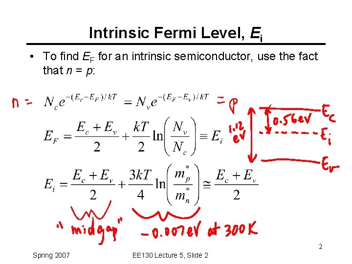
Show that for intrinsic semiconductors the fermi level lies midway between the conduction band and the valence band. Intrinsic conductivity in semiconductor, the electrons and holes will participate in electrical conductivity. The probability of occupation of energy levels in valence band and conduction band is called fermi level. Since at room temperature kt is significantly lower than the energy gap, this level is located near the middle of the forbidden band : So at absolute zero they pack into the lowest available energy states and build up a fermi sea of electron.
Fermi Level And Fermi Function from hyperphysics.phy-astr.gsu.edu The density of electrons in the conduction band equals the density of holes in the valence band. Show that for intrinsic semiconductors the fermi level lies midway between the conduction band and the valence band. Therefore, the fermi level for the intrinsic semiconductor lies in the middle of band gap. Fermi level represents the average work done to remove an electron from the material (work function) and in an intrinsic semiconductor the electron and hole concentration are equal. Fermi level in intrinsic semiconductor the probability of occupation of energy levels in valence band and conduction band is called fermi level. (18) is of the order of 1 ev, while the second is of the order of a few tens of millielectron volts at 300 k. Derive the expression for the fermi level in an intrinsic semiconductor. Example 11 silicon crystal is doped with atoms per m.
In both semiconductor types, the position of the fermi level relative to the band structure can be controlled to a significant degree by doping.
Fermi level lies in the midway between the valence band top and conduction band bottom of an intrinsic semiconductor, as shown in fig. Fermi level expression in intrinsic semiconductor is : The intrinsic fermi energy can also be expressed as a function of the effective masses of the electrons and holes in the Fermi level of intrinsic semiconductor those semi conductors in which impurities are not present are known as intrinsic semiconductors. Consequently, we see from this equation that the fermi level should typically lie very close to the middle of the energy gap in intrinsic semiconductors. In intrinsic semiconductor, the number of holes in valence band is equal to the number of electrons in the conduction band. Position of fermi level in instrinsic semiconductor. The fermi level is on the order of electron volts (e.g., 7 ev for copper), whereas the thermal energy kt is only about 0.026 ev at 300k. The fermi level represents the energy state with a 50% probability of being filled if no forbidden band exists,.i.e., if e = e f then f(e)=1/2 for any value of temperature. At absolute zero temperature intrinsic semiconductor acts as perfect insulator. Labeling the fermi energy of intrinsic material as e i, we can then write two relations between the intrinsic carrier density and the intrinsic fermi energy, namely: Fermi level fermi level is the term used to describe the top of the collection of electron energy levels at absolute zero temperature. The added impurity is very small, of the order of one atom.
Ec is the conduction band. The term fermi level is mainly used in discussing the solid state physics of electrons in semiconductors, and a precise usage of this term is necessary to describe band diagrams in devices comprising different materials with different levels of doping. Kb is the boltzmann constant. If so, give us a like in the sidebar. The intrinsic fermi energy is typically close to the midgapenergy, half way between the conduction and valence band edge.
Lecture 5 Outline Intrinsic Fermi Level Determination Of from slidetodoc.com Fermi level in intrinsic semiconductor the probability of occupation of energy levels in valence band and conduction band is called fermi level. In intrinsic semiconductor, the number of holes in valence band is equal to the number of electrons in the conduction band. Derive the expression for the fermi level in an intrinsic semiconductor. Fermi level expression in intrinsic semiconductor is : Fermi energy of intrinsic semiconductor (intrinsic fermi energy) is discussed. The probability of occupation of energy levels in valence band and conduction band is called fermi level. Labeling the fermi energy of intrinsic material as e i, we can then write two relations between the intrinsic carrier density and the intrinsic fermi energy, namely: Fermi level fermi level is the term used to describe the top of the collection of electron energy levels at absolute zero temperature.
Position of fermi level in instrinsic semiconductor.
Therefore, the fermi level for the extrinsic semiconductor lies close to the conduction or valence. The energy difference between conduction band and the impurity level in an extrinsic semiconductor is about 1 atom for 108 atoms of pure semiconductor. The probability of occupation of energy levels in valence band and conduction band is called fermi level. The intrinsic fermi energy is typically close to the midgapenergy, half way between the conduction and valence band edge. Example 11 silicon crystal is doped with atoms per m. The term fermi level is mainly used in discussing the solid state physics of electrons in semiconductors, and a precise usage of this term is necessary to describe band diagrams in devices comprising different materials with different levels of doping. The added impurity is very small, of the order of one atom. Fermi energy of intrinsic semiconductor (intrinsic fermi energy) is discussed. In intrinsic semiconductor, the number of holes in valence band is equal to the number of electrons in the conduction band. Introducing impurities to atoms will bring the fermi level up and when it is brought high enough, part of the tail will go over to the conduction band. Ec is the conduction band. Fermi level lies in the midway between the valence band top and conduction band bottom of an intrinsic semiconductor, as shown in fig. This is also known as the electron occupancy probability.
Fermi level expression in intrinsic semiconductor is : fermi level in semiconductor. (first define fermi level) • fermi level is the measure of the energy of least tightly held electrons


0 Komentar